 ©
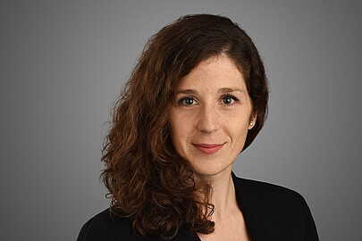
Mayra Garcés-Schröder
38106 Braunschweig

 ©
Mayra Garcés-Schröder
38106 Braunschweig
Who are you and what is the topic of your research group?
My name is Mayra Garcés-Schröder and we are investigating chip processing technologies for the production of active and passive micro- and nano-optical elements. These are, for example, arrays of gallium nitride-based LEDs, chip-integrated lasers and waveguides. The processing of materials such as gallium and aluminium nitride is often challenging due to their properties. We deal with the investigation of the different necessary manufacturing processes with regard to their influences on the material and component properties as well as their compatibility with each other.
Which research question are you working on?
How can chemically and mechanically stable compounds such as gallium and aluminium nitride be processed carefully so that their highly interesting properties for photonics are retained and challenging architectures are nevertheless made possible? Which materials are suitable for masking the layers in different processes and how can we increase the reliability and reproducibility of our manufacturing processes? An important question is also the compatibility of our manufacturing processes and elements with those of other disciplines in order to create added value there with integrated optics.
What makes this topic special/exciting for you?
The development and implementation of innovative system architectures for various applications is always exciting and demands creativity and openness to unconventional approaches as well as systematic work and critical analysis. I find it very fascinating to think of a solution to a processing problem and in the end - often after many setbacks - to see a tiny, functional component in the scanning electron microscope as the result.
How does your topic help to push the boundaries of what can be measured?
We are working on two different frontier shifts.
On the one hand, we are working towards integrating small light sources directly on other chips, for example for gas sensors, particle detection or point-of-care diagnostics, thus making measuring devices much more widely available. This makes it conceivable to take a miniaturised laboratory to remote areas, so to speak, and carry out analyses there. On the other hand, miniaturisation and mass production can lead to the development of cheaper sensors that can then be used in large numbers on a large scale.
On the other hand, we work in interdisciplinary projects with biologists and pharmacists, for example, who can illuminate cells or even cell components very locally and thus very carefully with our micro-LEDs. If the cells are pre-treated accordingly, certain processes can be triggered. In this way, the development of diseases or the mechanism of action of drugs can be investigated at the cellular level.
What is special about participating in the QuantumFrontiers cluster of excellence?
QuantumFrontiers bundles the competences of several locations and disciplines, which on the one hand enables the members to think outside the box and get to know fields of work they would otherwise not encounter in everyday life. On the other hand, the diversity of the equipment available as a result is impressive. There are numerous opportunities to network with other members of the cluster and to learn a lot through scientific exchange. The open structures and uncomplicated interaction within the cluster make it easier to get into conversation with the other scientists and discuss ideas or challenges.


